Details of test chip designs: pad pitch, layout, materials, and opening.
![Details of test chip designs: pad pitch, layout, materials, and opening.](https://www.researchgate.net/publication/28578026/figure/fig1/AS:670717242773506@1536922860459/Details-of-test-chip-designs-pad-pitch-layout-materials-and-opening.png)
![](https://upload.wikimedia.org/wikipedia/commons/thumb/3/3e/Nordic-NRF24L01P-HD.jpg/300px-Nordic-NRF24L01P-HD.jpg)
Chip Design Made Easy - Wikibooks, open books for an open world
![](https://image.slidesharecdn.com/apex2013padcrateringtutorial-140824083059-phpapp01/85/pad-cratering-prevention-mitigation-and-detection-strategies-3-320.jpg?cb=1668023613)
Pad Cratering: Prevention, Mitigation and Detection Strategies
What is Pad to Pad (PP) in PCB ?. Pad to Pad or PP is an important
![](https://preview.redd.it/pcb-review-request-review-for-prototype-pcb-built-around-v0-ycswnmnhz18a1.png?width=1482&format=png&auto=webp&s=90414d4d70e65f5164ea596a81ba0d3321bba716)
PCB Review Request] Review for prototype PCB built around MAX86171
![](https://www.researchgate.net/publication/237062038/figure/fig1/AS:299435969007621@1448402506590/Upper-part-Layout-of-the-flip-chip-with-60-mm-solder-spheres-applied-on-the-outer-row.png)
Upper part: Layout of the flip-chip with 60 μm solder spheres applied
Ball Grid Array Technology Overview
![](https://d36ae2cxtn9mcr.cloudfront.net/wp-content/uploads/2023/07/21054838/Sk-hynix_semiconductor-back-end-process-ep5_02.png)
Semiconductor Back-End Process 5:Package Design and Analysis
![](https://semiengineering.com/wp-content/uploads/Fig04_FlipChip_diagram_SE_AM-e1684372087642.png)
Challenges Grow For Creating Smaller Bumps For Flip Chips
![](https://www.protoexpress.com/blog/wp-content/uploads/2021/03/NSMD-pad.png)
What is a Pad in PCB Design and Development
![](https://img.yumpu.com/21864272/1/500x640/fine-pitch-flip-chip-with-cu-pillar.jpg)
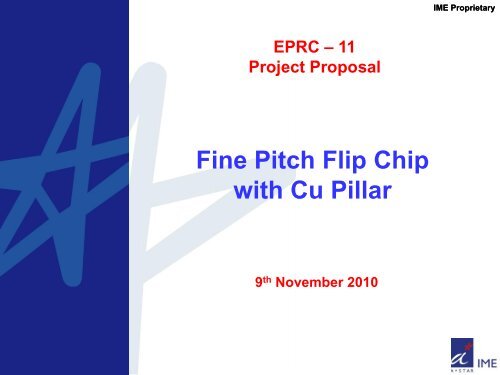
Fine Pitch Flip Chip with Cu Pillar
![](https://anysilicon.com/wp-content/uploads/2018/06/img_5b1c107e83b09.png)
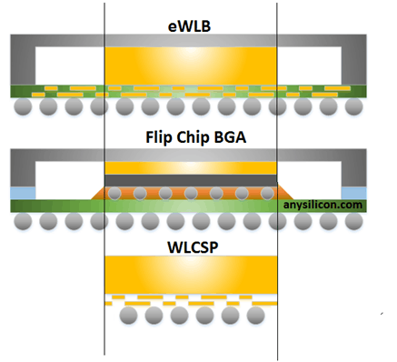
Understanding Wafer Bumping Packaging Technology - AnySilicon
![](https://www.analog.com/en/_/media/analog/en/landing-pages/technical-articles/pcb-design-considerations-and-guidelines-for-04mm-and-05mm-wlps/5283fig03.gif?rev=3851adedfdf74c4faf6d2fa6bfc3e4f8)
PCB Design Considerations and Guidelines for 0.4mm and 0.5mm WLPs
![](https://ars.els-cdn.com/content/image/1-s2.0-S2772671122000249-gr7.jpg)
Challenges and recent prospectives of 3D heterogeneous integration
![](https://ars.els-cdn.com/content/image/1-s2.0-S2772671122000249-gr9.jpg)
Challenges and recent prospectives of 3D heterogeneous integration - ScienceDirect