PDF] Design and Fabrication of Bond Pads for Flip-Chip Bonding of Custom Dies to CMOS Dies
![PDF] Design and Fabrication of Bond Pads for Flip-Chip Bonding of Custom Dies to CMOS Dies](https://d3i71xaburhd42.cloudfront.net/81ca422bb36b6d17a1e9deb91b8b7e477e72afab/3-Figure2-1.png)

George Harman - WIRE BONDING IN MICROELECTRONICS, 3 - E (2010, McGraw-Hill Professional) PDF, PDF, Materials

PDF) Direct flip-chip bonding of bare dies to polypropylene-coated paper substrates without adhesives or solders

Digital Design
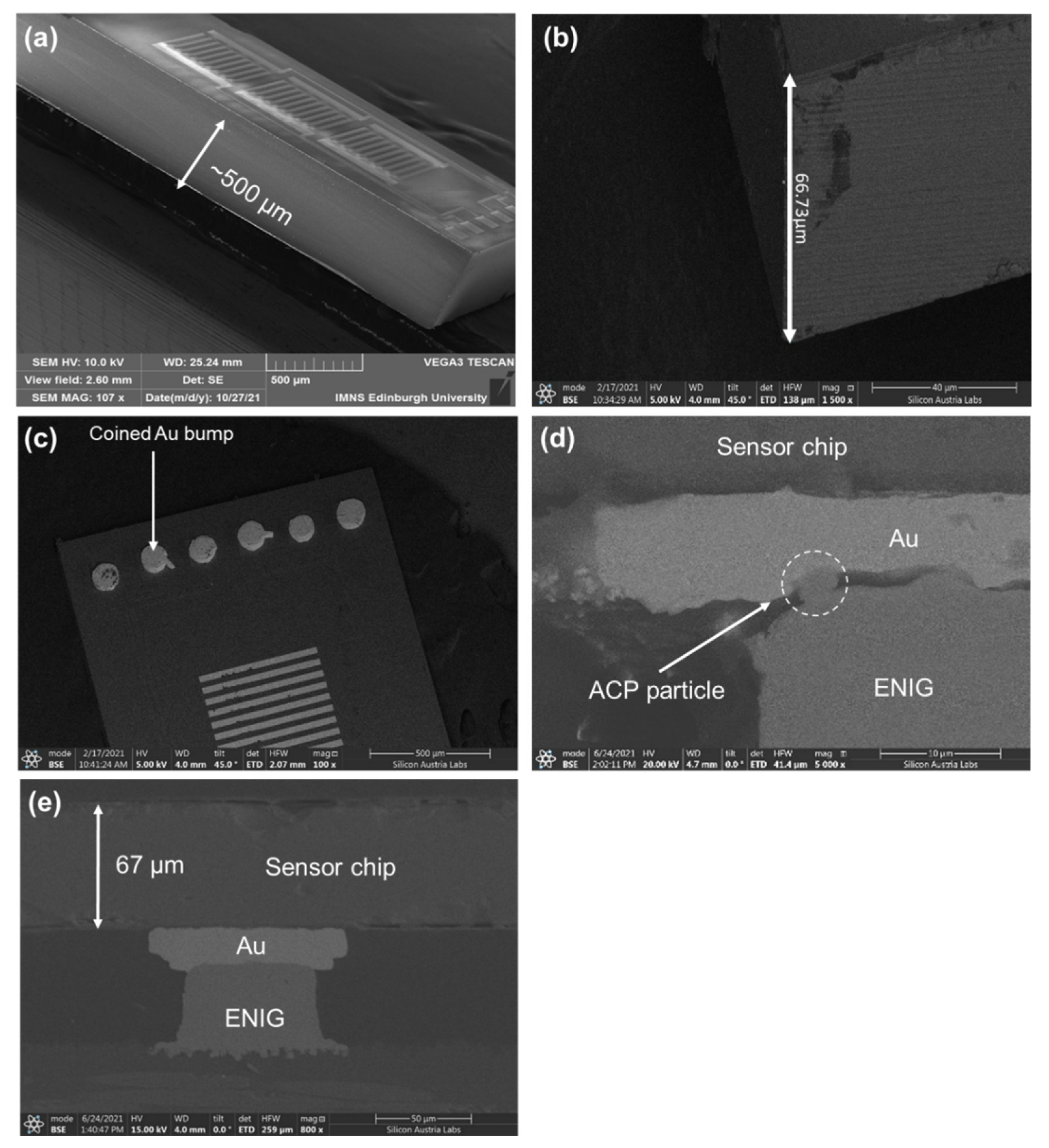
Electronics, Free Full-Text

PDF] Design and Fabrication of Vertically-Integrated CMOS Image

Flip-Chip Packaging for Nanoscale Silicon Logic Devices

Semiconductor device fabrication - Wikipedia

PDF] Design and Fabrication of Bond Pads for Flip-Chip Bonding of

State-Of-The-Art of Advanced Packaging
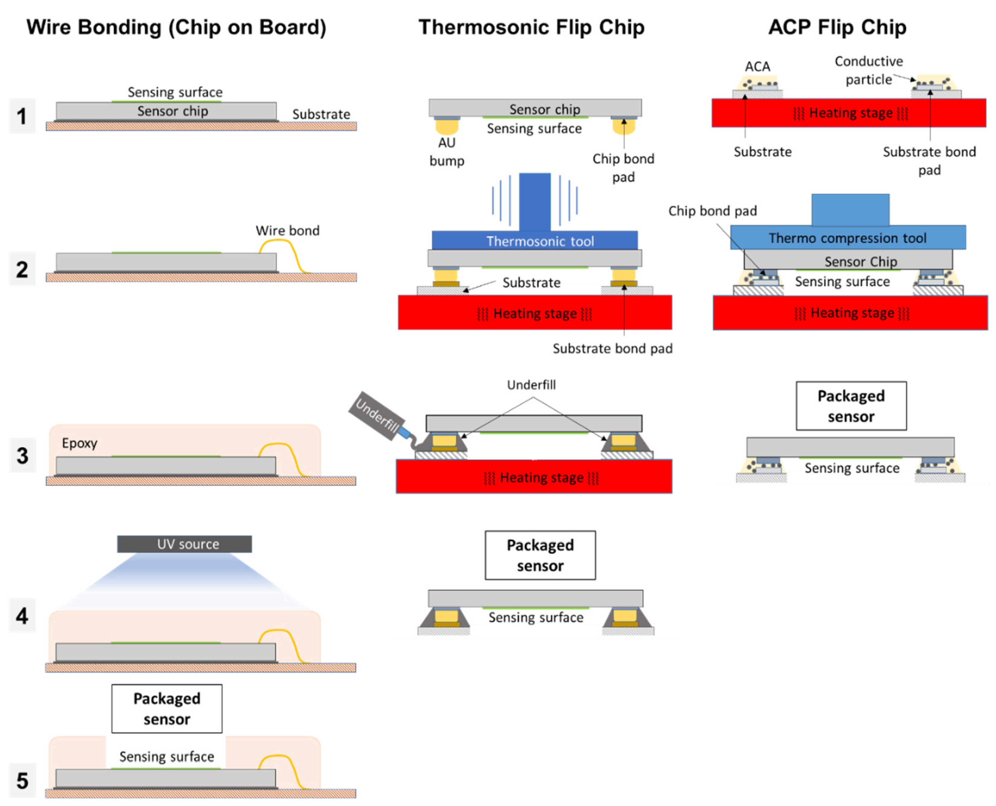
Electronics, Free Full-Text
You may also like


Related products