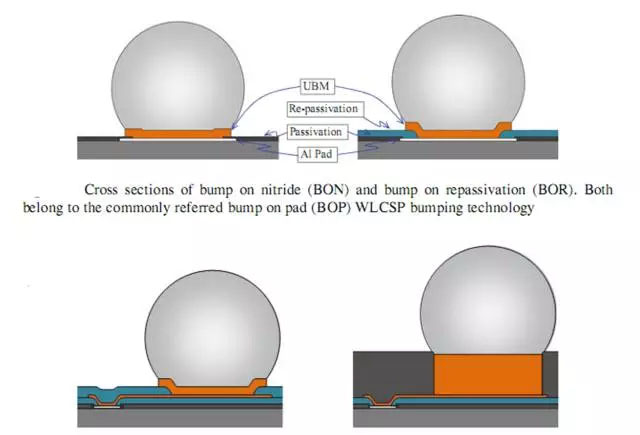
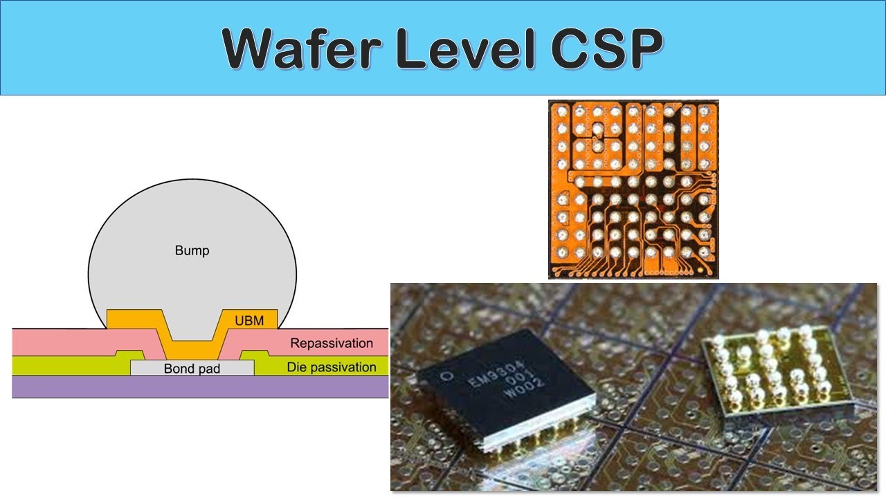
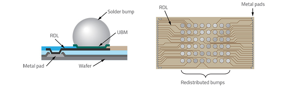
Bump on Pad, Wafer Process Technology
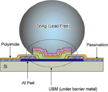
Bump on Pad Key features include: Wafer process and bumping in consolidated assembly. Technology supporting wide range of products from mobile devices to
NEWS - Strong Electronics&Technology Limited
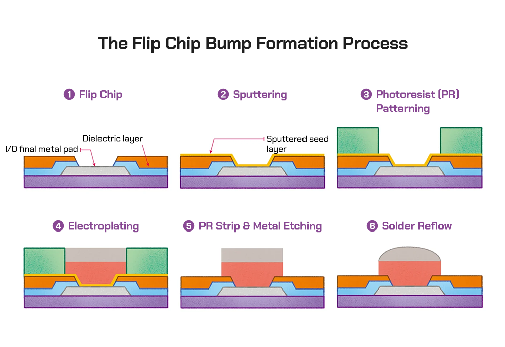
Wafer bumping process sequence.
Eng Sub] Wafer Level Chip Scale Package (WLCSP)

Micromachines, Free Full-Text

PDF] Modeling a low cost wafer bumping technique for Flip Chip application
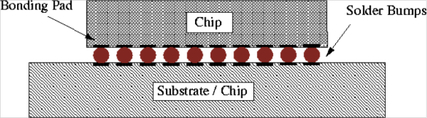
Solder Bump Bonding, Ball Bumps and Wire Bonds
Tech Brief: Primer on Packaging
)
Prestige Popular Stainless Steel Pressure Cooker, Litres
d36ae2cxtn9mcr.cloudfront.net/wp-content/uploads/2
Wafer with pad, bumps and daisy chain partial layout (quarter of die

Status and Outlooks of Flip Chip Technology
ChipMOS TECHNOLOGIES INC. – Back-end testing service for memory, LCD Diver, Bumping and MEMS.

BumpJiangsu CAS Microelectronics Integration Technology Co Ltd
Wafer Bumping Machines for Assembly Process Interconnections